The Indian Nanoelectronics Users’ Program (INUP), at IISc and IIT Bombay, is training researchers across the country to build national capability in nanoelectronics
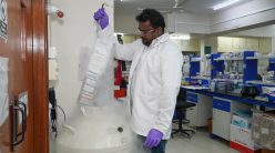
Since it began in 2008, the Indian Nanoelectronics Users’ Program (INUP) has received exceptional positive feedback from its participants. Among them are college teachers who say that their participation in the training programme helped them become better teachers because they had the opportunity, for the first time, to handle silicon wafers – the critical component used to fabricate the innards of electronic devices.
“This was a completely unanticipated benefit,” says SA Shivashankar, a visiting professor at the Centre for Nano Science and Engineering (CeNSE), IISc. “It wasn’t a part of our proposal at all.” (Shivashankar was the Principal Investigator for INUP until he retired in 2012.)
College teachers say that their participation in the training programme helped them become better teachers because they had the opportunity, for the first time, to handle silicon wafers
The idea behind INUP is simple: The state-of-the-art facilities and the expertise at CeNSE would be made available to the wider research community in India to work on their ideas. These are projects they would otherwise have been unable to work on because they didn’t have access to the facilities nor the training to use them.
INUP is part of a larger effort to meet the goals of the National Policy in Electronics: to build up national capabilities for a larger electronics R&D and industry base that can serve the domestic and export markets rather than having to rely on imports. “We [India] missed the bus for the microelectronics revolution. The government didn’t want it to happen for nanoelectronics too,” says Navakanta Bhat, Chairperson of CeNSE and the present Principal Investigator of INUP. “The aim is to create human resources in this area, a critical mass of people who can contribute. This will create a ‘multiplier effect’, where the people we train will go out and influence others.”
INUP is supported by the Ministry of Electronics and Information Technology which funded the Centres of Excellence in Nanoelectronics at IISc and IIT Bombay. These two institutions were then tasked with implementing INUP, making available their facilities to researchers from around the country.
The three-level programme is open to PhD students and faculty members at institutions across India. For the Level 1 Familiarization Workshop, about 100 participants attend lectures for three days, and get an introductory tour of the facilities at CeNSE. These are participants who, as part of the application process, have submitted a poster outlining a proposal for research using the facilities at CeNSE. Over the years, it was found that participation from certain parts of India, such as the northeastern states, was low, which prompted proactive seeking of participants from these regions by conducting Level 1 programs there. Such outstation workshops, which have been conducted in Uttarakhand and Rajasthan too, now form one of about half-a-dozen Level 1 workshops offered each year.
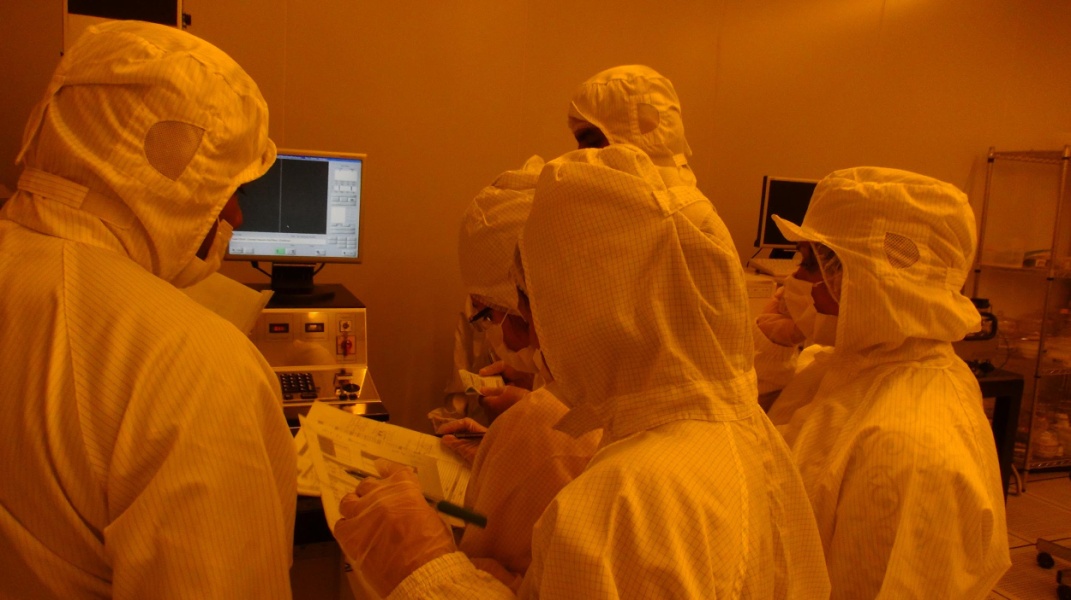
Participants who have attended a Level 1 course, or who are otherwise eligible, attend a Level 2 Hands-on Training workshop at the facilities at CeNSE. This is a two-week programme for about 30 participants, consisting of four modules: on MEMS/NEMS (micro/nano-electromechanical systems) fabrication, nanoelectronics fabrication, photovoltaics, and gas sensors. These modules are run in parallel with five to seven participants each, training them on the tools that can be used to realise their research proposal. CeNSE is especially suited for such training, given the facilities it has for everything from fabrication to packaging, not usually found together, in the form of the National Nanofabrication Facility, the Micro and Nano Characterization Facility, the System Engineering Facilty, and the MEMS & IC Packaging Facility. “These facilities at IISc are comparable to the best in the world,” says Bhat.
“These facilities at IISc are comparable to the best in the world”
At the end of the Level 2 workshop, the participants have to make a presentation with a detailed research proposal, where they receive feedback from faculty members and technical staff at CeNSE. “Based on these inputs and the training they have received, they may have to modify their research proposals, and members of faculty and the technical staff here help them do that,” says Sanjeev Kumar Shrivastava, Coordinator and Technology Manager of INUP. They then have to resubmit their proposals, which are evaluated by a committee. Some are asked to modify their research proposal further, and selected participants come back to work on their proposed project – the third level of the programme. “At any point of time, there are one or two people here doing long-term projects,” says Shrivastava.
In its Phase I, from 2008 to 2014, INUP exceeded its targets. It is currently in its Phase II, which will last till 2019 – but the targets have been met in just two years. So far, INUP has trained more than 4200 researchers from 450 institutions across India, covering a wide swath of institutions, including some of the IITs and NITs. Many participants come from smaller, lesser-known, private engineering colleges, some of whom have gone on to file for patents for their work. This has resulted in more than 250 PhD theses based partly or wholly on work done through INUP at CeNSE; it has also resulted in about 210 published papers and 17 patents filed/awarded. The projects they have worked on range from synthesis of nanomaterials and nanostructures to fabrication of nanodevices and characterisation of their performance.
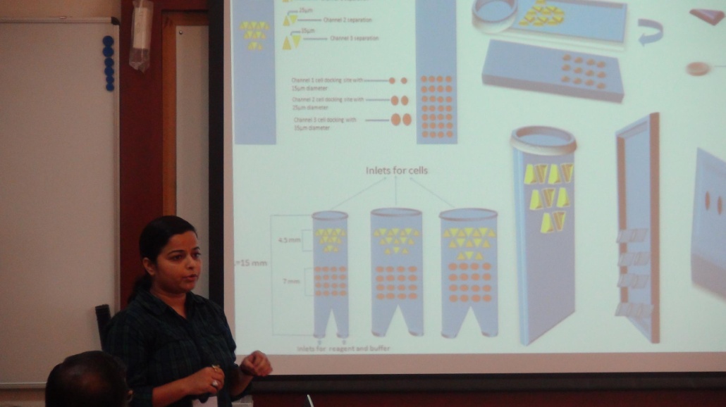
All this work means that more than a dozen papers are published every year as part of INUP, none of which have IISc faculty as co-authors, a deliberate policy. “It is their work. They have taken the initiative and put in the work,” says Bhat.
The training programme has now been offered for researchers from India’s neighbouring countries too – such as Sri Lanka, Bangladesh, Myanmar, Maldives, Vietnam, Kazakhstan – through the Indian Technical and Economic Cooperation (ITEC) programme of the Ministry of External Affairs. Further, India’s experience with INUP was presented at the University/Government/Industry Micro/Nanotechnology (UGIM) Symposium – a prominent conference in the field of micro/nanotechnology – where, Bhat says, representatives from other countries expressed interest in replicating this programme. Unlike other such networked training programmes elsewhere in the world, participants of INUP – who may find it difficult to obtain research grants – do not have to pay for access to the facilities. In fact, their travel and accommodation costs too are taken care of. “This frees them up to focus on their work here,” says Bhat. They also get to tap the expertise of faculty members at IISc.
Unlike other such networked training programmes elsewhere in the world, participants of INUP – who may find it difficult to obtain research grants – do not have to pay for access to the facilities.
Through its website, INUP has made efforts to network its participants with one another and with prospective participants. A student or faculty from a particular institution, for instance, can look up who else has participated from their region and get to know what kinds of projects have been implemented.
Based mostly on word-of-mouth communication, INUP has seen an increasing number of applicants over the years. “Its popularity, with the increasing participation, shows that it’s been a resounding success,” says Shivashankar.

