A deep dive into the evolution of the microscope that has enabled groundbreaking discoveries
In my eighth grade classroom, amidst sunbeams dancing on dusty desks, the creaking sound of the ceiling fan, and the pungent smell of chemicals, my science teacher Deepak Sah’s words painted a universe where tiny things held big secrets. We learned about simple and compound light microscopes capable of revealing worlds invisible to the naked eye. “But wait, there’s more!” he’d say with a wink. “There are electron microscopes that use electrons instead of light to increase the resolution further.” A fascination for these magical machines took root in my mind. But I had many questions. What did resolution mean? Why electrons and not light?
It took me several years to learn some of the answers. I learned that resolution is the smallest gap between two points before they blur together. Our eyes max out at a resolution of around 0.1 mm, roughly the thickness of a fine spiderweb. A trusty light microscope could stretch that to 0.3 micrometres – a thousand times higher resolution – enough to reveal the hidden world within a grain of sand. But even this machine can’t catch the dance of atoms – about 3,000 times smaller – which drives almost all material properties, from strength to magnetism to superconductivity.
Zooming into the atomic level isn’t just about magnification. In 1879, English mathematician Lord Rayleigh showed that the resolution limit depends directly on the wavelength (“size” or “step”) of the light shined on the object and inversely on the microscope’s numerical aperture. Like a detective’s ability to discern footprints based on boot size, the microscope’s capability to resolve fine features was directly tied to the wavelength of light it used. Even the most powerful light microscopes are limited because visible light exists only at long wavelengths, much larger than the size of atoms.
In 1925, French physicist Louis de Broglie proposed an audacious idea: Particles like electrons can also behave like a wave, with wavelength inversely proportional to the square root of its energy. If electron beams are given an energy boost, their steps (wavelengths) would shrink, improving resolution drastically, turning these electrons into nimble nanoscale detectives. By firing high-energy electrons at an object and tracking their scattering and/or absorption, scientists can map out an object’s structure down to atomic arrangements.
By firing high-energy electrons at an object and tracking their scattering and/or absorption, scientists can map out an object’s structure down to atomic arrangements
During my second year of Integrated PhD at IISc, I came to learn about different types of electron microscopes. There are Transmission Electron Microscopes (TEMs), which fire electrons at samples to peer at their interior, and Scanning Electron Microscopes (SEMs), which scan surfaces to create 3D images. TEMs generally have higher resolution. However, compared to SEMs, they are typically more complex, expensive, and require specialised sample preparation.
“The origins of electron microscopy can be traced back to groundbreaking work of German physicists Ernst Ruska and Max Knoll in the 1930s when they created the first TEMs,” says Pavan Nukala, Assistant Professor in the Centre for Nano Science and Engineering (CeNSE), IISc. “After that, the name of the game has always been to improve the resolution.”
Boosting resolution
In the beginning, there were two main strategies for improving resolution – decreasing the wavelength of electrons or increasing the TEM’s numerical aperture. Decreasing the wavelength centred on boosting the energy of electrons, starting from 100 KeV TEMs and going up to two-storey-tall TEMs capable of firing electrons at 2,000 KeV. But this proved problematic. “This brute-force approach posed challenges because materials couldn’t always withstand these very energetic electrons,” explains Pavan. “[Scientists] realised that these electrons could even damage specimens and alter the surface morphology of materials under study.”
Soon, scientists shifted their attention to the numerical aperture. Increasing it allowed more electrons to be collected and enabled the use of smaller probes. However, larger apertures introduced imperfections in image quality, like colour fringes, blurs, and distortions.
Subsequent breakthroughs focused on developing aberration correctors. These correctors use complex algorithms and electromagnetic lenses to “undo” lens-induced aberrations in real-time. This correction significantly enhances imaging clarity, precisely manipulating the electron beam to focus more accurately on nanoscale structures and materials, even with low-energy electrons.
But by the 2000s, attempts to correct aberrations plateaued, just like the very high-voltage TEMs.
Finally, researchers decided to focus on improving the detectors – enhancing the signal-to-noise ratio of the obtained data. Modern detectors are quite sensitive and capable of capturing a broad range of electron signals, allowing for better image contrast and detail. Together, these innovations have propelled electron microscopy to unprecedented levels of resolution and clarity.
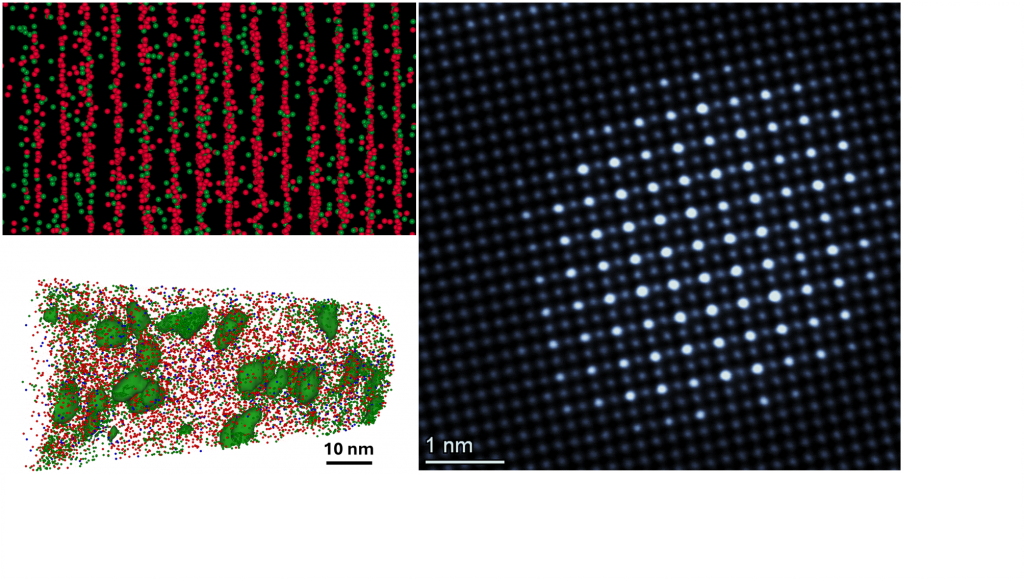
“These advancements have pushed the boundaries to the extent where resolutions as fine as 20 picometers [one-trillionth of a metre] have been achieved and documented in the Guinness World Records,” says Pavan. “It serves as a testament to the remarkable progress made in electron microscopy.”
Current efforts in the TEM world are directed towards sample holders, explains Surendra Kumar Makineni, Assistant Professor at the Department of Materials Engineering (MTE). Specialised liquid cell holders allow scientists to watch a chemical reaction like corrosion or oxidation unfold like a live performance in incredible detail. Holders that can strain the sample and provide electric and magnetic biases let scientists see how materials behave under electric or magnetic fields at the atomic scale.
Advancements are also happening in sample preparation. Traditional methods like polishing and ion milling can introduce unwanted artefacts that hinder a clear view. Focused Ion Beam (FIB) techniques are better. But gallium ions, commonly used in FIBs, can still interact with the material, leaving artefacts behind. The latest breakthrough in sample preparation is plasma FIBs utilising xenon sources. Xenon interacts very little with most materials, resulting in samples with significantly less damage and offering a much clearer view of the underlying structures. Instruments like Energy Dispersive X-ray Spectroscopy and Wavelength Dispersive Spectroscopy that work in tandem with TEMs are also allowing scientists to identify elements quickly and efficiently.
Costs and challenges
How much does a TEM cost? This was another question that came to mind when I started using them for my PhD.
“The typical cost of cutting-edge TEM can vary, usually around Rs 15-20 crore, depending on specifications,” Pavan answered. “Funding for a TEM can be challenging, especially for individual labs. I wouldn’t want to buy a TEM for myself and keep it in my lab just to do my research. It’s often managed as a central facility to maximise accessibility, which is the best use of taxpayer’s money.”
As a trainee, I also realised that operating a TEM is quite challenging compared to other instruments. Pavan points to a common misconception about TEM. Many users, he says, view it as a daunting “black box”. There may be some logic to this fear, given the costs involved with what appear to be genuine mistakes. As a result, one needs to deeply understand how it works to be able to operate it safely and to its full potential, which is an activation barrier for people. “However, with advancements in automation, the robustness against human errors is increasing. So, administrators can relax a bit from the erstwhile mentality and create confidence-building measures, as well as an environment where TEMs are democratised and used without fear,” adds Pavan.
Pavan points to a common misconception about TEM. Many users, he says, view it as a daunting “black box”
In a research institute like IISc, maintaining behemoths like TEMs is no small feat. There are constant interactions between the Institute and vendors supplying these machines. Dedicated technicians are the first responders who keep running these instruments smoothly.
About 95% of technical issues – small repairs and replacements – can be resolved locally, Pavan says. However, for the trickier 5%, expertise from abroad might be needed, which can add to the budget. This responsibility falls on faculty members, who juggle research with ensuring these tools keep generating valuable data.
One way to offset these extra costs is by charging for facility use. This helps cover maintenance costs and allows the Institute to hire dedicated staff instead of relying on temporary student operators. In the long term, there is a need to create a culture where everyone, from researchers to technicians, contributes to keeping these instruments in top shape, Pavan says.
TEM at IISc
“The microscopy tradition at IISc is the [microscopy] tradition of India,” says Kamanio Chattopadhyay, Emeritus Professor and National Science Chair at MTE.
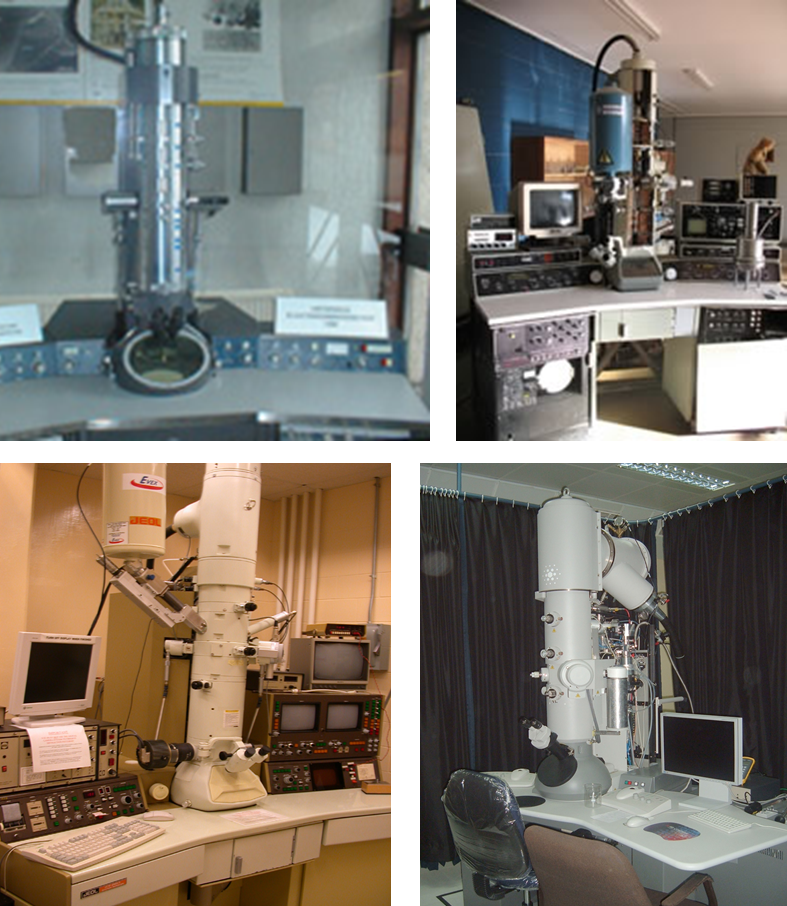
Although the first TEM microscope was built in the late 1930s, it did not become commercially available until 1949. Till then, researchers built their own. “The first microscope in the history of Indian science was built at Calcutta University by NN Das Gupta in 1947-48,” recalls Kamanio. One of Das Gupta’s close associates, DL Bhattacharya, joined IISc in the early 1950s. It was then that IISc decided to buy the Philips EM100, one of the first commercial TEMs ever built, launched in 1949. It was processed in 1951-1952 and installed on the ground floor of the Department of Metallurgy (later MTE). “I do not know where that microscope went,” Kamanio adds. “I tried hard to find it when I came to IISc in 1981 … it was probably melted down.”
In 1978, the Institute procured a Philips EM300, the latest at the time. It was also briefly installed in the Department of Metallurgy and later moved to the new building of the Materials Research Laboratory (MRL) after it became ready. In 1982, faculty members led by CNR Rao and S Ranganathan secured funds to purchase the JEOL 200CX and asked Kamanio and Subbanna, a scientific officer, to set it up in MRL. “Subbanna’s contribution was tremendous,” reminisces Kamanio.
MRL became the Materials Research Centre (MRC) in 1987, and the demand for microscope time increased. “We had some difficulty, at least in metallurgy, because we were doing a lot of work,” Kamanio says. In 1990, he and Ranganathan managed to buy the JEOL 2000 FX II, which served well into 2015.
In the early 1950s … IISc decided to buy the Philips EM100, one of the first commercial TEMs ever built
In 2001, M Vijayan, the then Associate Director, asked Kamanio, Chair of MRC at that time, to set up a cutting-edge TEM (the Tecnai F-30 FEI microscope) at the Institute. It was an initiative of IISc with matching funds from the Department of Science and Technology. At that time, faculty members Sanjay Biswas from the Department of Mechanical Engineering and Vikram Jayaram from MTE got a grant for a Focused Ion Beam microscope. The Institute also received funds for an SEM from the Nano Mission. It was suggested that all these microscopes should be kept together, which was supported by Goverdhan Mehta, the then Director. An old residential building was identified near the BSNL telephone exchange and renovated due to the efforts of Kamanio, Subbanna, Vikram and Arup Kumar Raychaudhuri. Called the Institute Nanoscience Initiative (INI), it was inaugurated in 2003. “Unfortunately, Subbanna did not live to see the centre start,” Kamanio says.
After INI was inaugurated, two new TEMs arrived, including the high-resolution T20 (Tecnai, FEI) and F30, Surendra recounts. With 200 KV and a thermal emission source, the T20 offered solid performance. The F30, packing a 300 KV punch and a field emission source, boasted even higher resolution due to its more focused electron beam. Notably, it could also switch to a scanning mode.
N Ravishankar, Professor at MRC, then secured funding through the Swarna Jayanti Foundation for another TEM – the ST20 (Tecnai, FEI) – and decided to place it at INI instead of his own lab. It offered functionalities similar to the T20. However, none of the microscopes had an aberration corrector. The T20 wasn’t destined for a very long life. Lens issues forced its decommissioning within a few years.
In 2010, the INI was renamed as the Advanced Facility for Microscopy and Microanalysis (AFMM) with the mandate to develop an ecosystem to facilitate the study of the structure and chemistry of materials at the atomic scale. Its goal is to develop manpower and capacities to carry out cutting-edge research by continuous development and training.
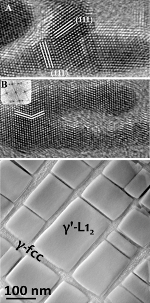
In the first decade of this century, the microscope world saw rapid developments, including aberration-corrected lenses and beam monochromators. This led to the arrival of a new champion – the Titan (300 kV Themis, FEI), a very expensive tool. Realising the importance and associated funding difficulties, P Balaram, the then Director, decided to fund the basic microscope from internal resources. Further funding from DRDO, due to the efforts of faculty member Dipankar Banerjee, upgraded its abilities with a monochromator – to ensure that only one electron wavelength interacts with the sample for razor-sharp resolution – and a probe corrector – to account for aberration, eliminating any beam imperfections for atomic-level imaging. Additionally, its electron energy loss spectroscopy (EELS) capability allowed precise detection of lighter elements. Integrated differential phase contrast (IDPC) imaging has recently been installed in the Titan, further enhancing light element mapping. A super Energy Dispersive X-ray Spectroscope (EDS) now rounds out its impressive arsenal, making it a dream tool for mapping individual atomic column compositions. Additionally, for atomic scale compositional analysis and 3D tomography, a state-of-the-art atom probe (LEAP 5000 XHR) was also procured in 2017 that boosted the AFMM capabilities in material characterisation.
CeNSE also recently acquired a Titan microscope, but without the aberration corrector, placing it closer to the AFMM’s F-30 in capabilities. However, it is a great tool to image nanoparticles. Today, these microscopes hum with activity, serving both IISc researchers and external partners.
Enabling breakthroughs
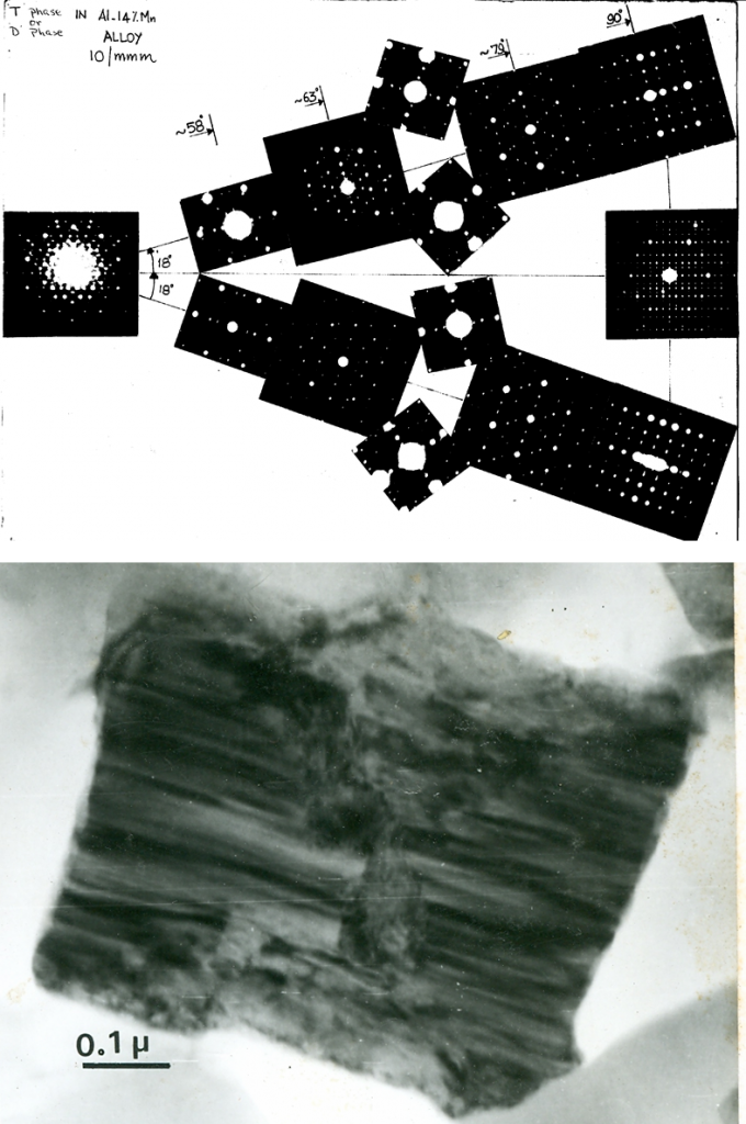
For decades, these microscopes have helped scientists at IISc make groundbreaking discoveries. For example, quasicrystals, which led to a 2011 Nobel Prize in Chemistry, were discovered in 1984 by Dan Schechtman at the National Bureau of Standards, Washington. “Within three months of that, we discovered decagonal quasicrystals, only because of the Philips 300,” Kamanio says. Other contributions include the discovery of superheating during phase transformation in the 1990s and work on nanowires by Ravishankar in the early 2000s, he adds.
Surendra recalls another instance. In 2010, when he was a PhD student under Kamanio, he stumbled across a research paper describing a promising cobalt-tungsten superalloy. It offered impressive strength and heat resistance, surpassing traditional nickel-based alloys used in jet turbines. However, its high tungsten content made it heavy and impractical for real-world applications.
Surendra, along with Nithin Baler, an MTech student, started scouring the periodic table for alternatives. Molybdenum emerged as a candidate, but not on its own. The breakthrough came when they added a small amount of niobium to it (cobalt-aluminium-molybdenum-niobium) – the microstructure stabilised, significantly reducing weight without sacrificing performance.
One late night, peering at the new material through the F30 TEM at AFMM, they saw that it showed the exact cubic structure as the original tungsten-based alloy, validating their intuition and theoretical predictions. Excited, Surendra called Kamanio at 1 am and informed him of the discovery. “Nobody thought that such an alloy could exist,” Kamanio recalls. The very next day, they started writing the manuscript. After some difficulties, the paper was finally published in 2015. The discovery sparked significant interest in the scientific community and even secured a research grant of Rs 5 crore from DRDO for the lab.
The microscopes at IISc have also helped train generations of budding scientists, Kamanio points out. “If you go anywhere in India and look at people doing microscopy, chances are that many of them were trained here,” he says. “TEM at IISc has a legacy dating back to the 1950s. And that is something which no place else has.”
Vivek Kumar is an Integrated PhD student in the Department of Physics, IISc and a science writing intern at the Office of Communications