India needs the right technology and policy to realise a gallium nitride future

Harshada Ahire was caught off guard as she opened the door of the Power Electronics Laboratory in the Department of Electrical Engineering (EE) at IISc, as I stepped into the large room. I was with Vinod John, Professor at EE, and Utsab Kundu, an INSPIRE faculty fellow. Tables along the walls had wires of different colours connected to a screen displaying voltage.
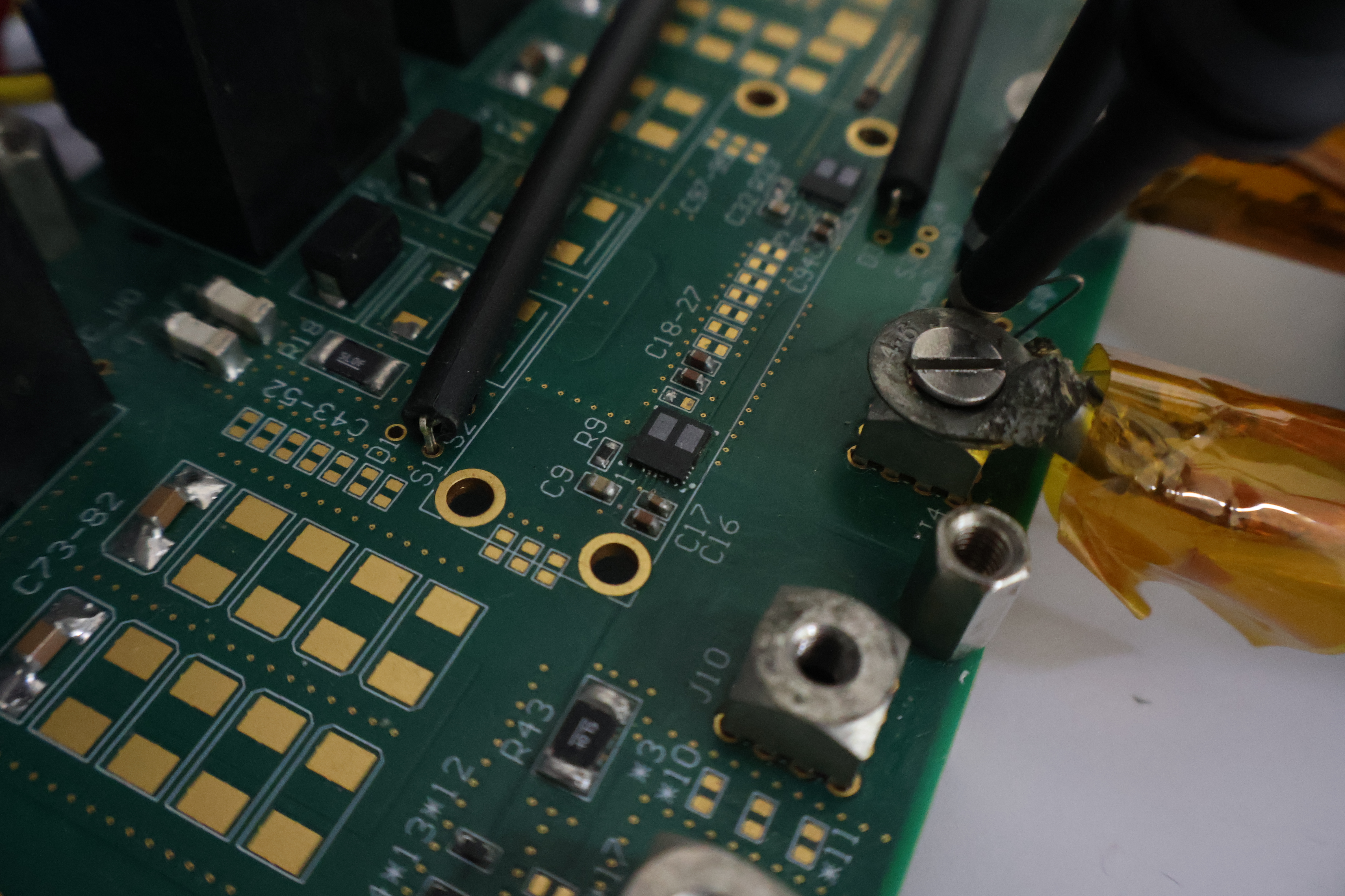
At one of the tables, Harshada, an MTech student, was working on a green board with tiny multicoloured devices; some cylindrical, some spherical, and some that looked misshapen.
“Do you see that tiny black device?” Vinod asked, drawing my attention to a thin black square on the board. “That’s it: the GaN [gallium nitride] transistor.”
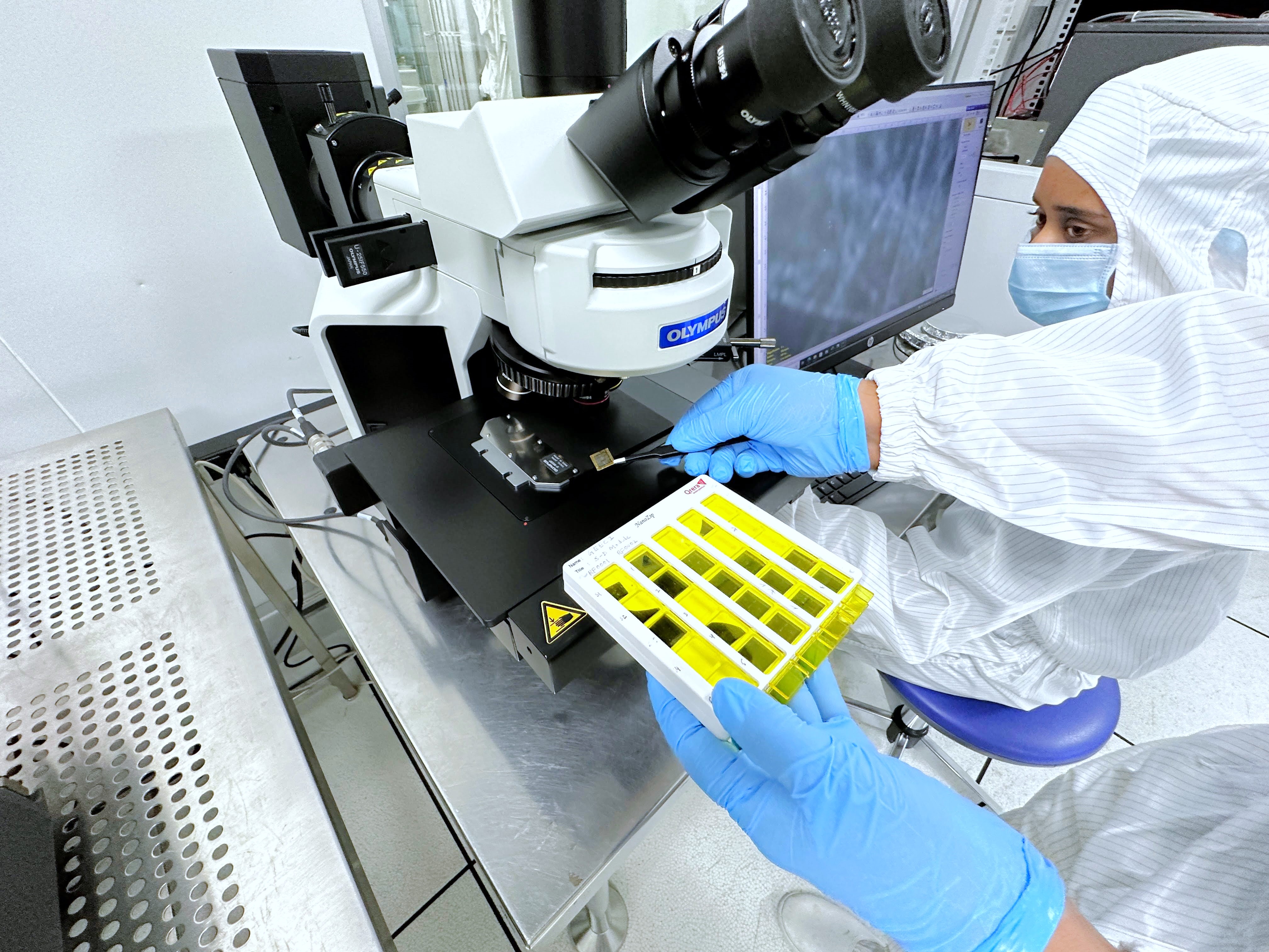
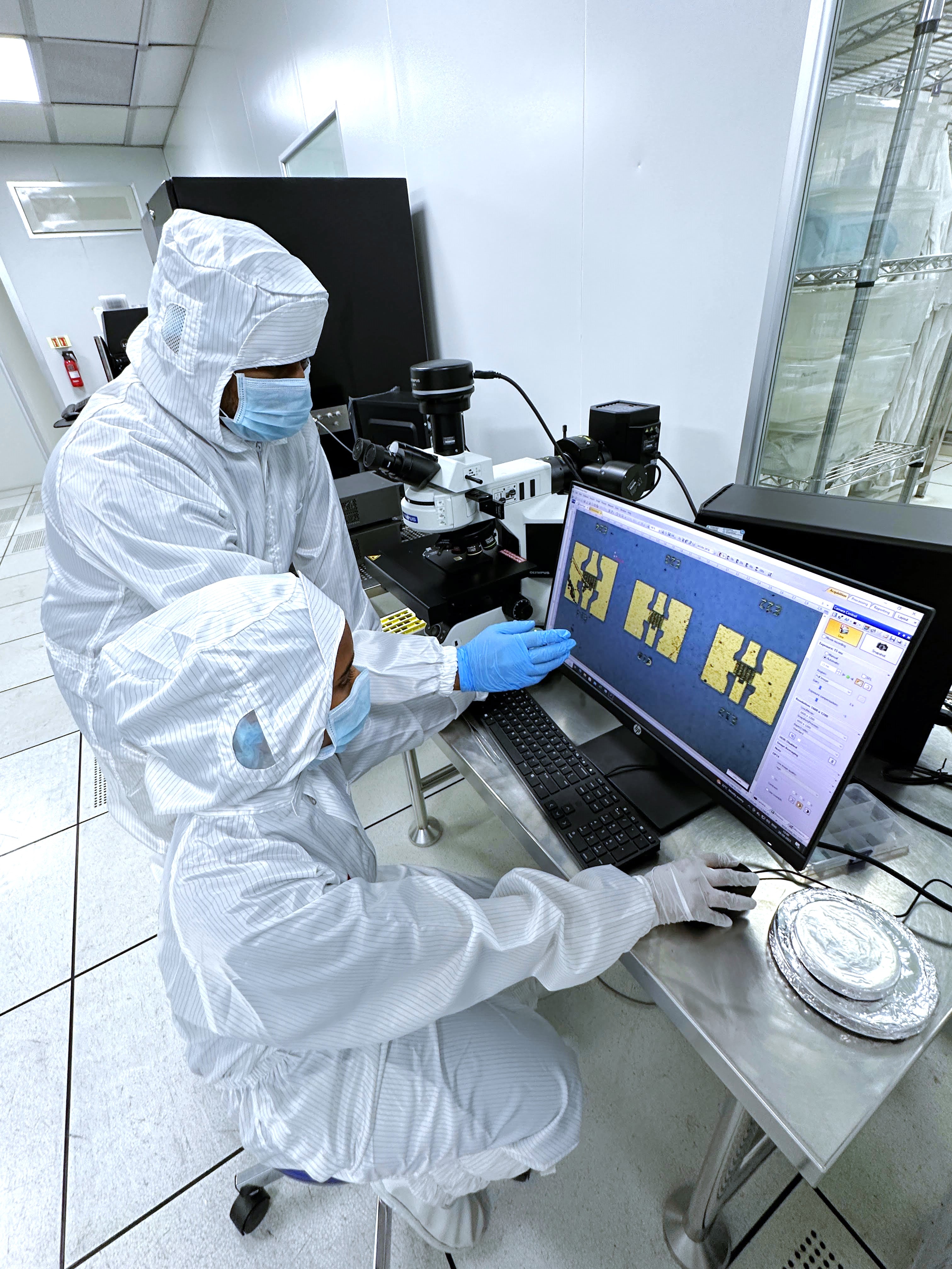
I had previously seen GaN wafers in an infant form, appearing with thin black lines on a lightweight circular disk, in the corridor of the clean room at the Centre for Nano Science and Engineering (CeNSE). Back in 2006, CeNSE served as ground zero for the growth of GaN research at IISc, says Srinivasan Raghavan, its Chair. Since then, several advances have been made in bringing GaN devices closer to reality.
Here and now in the Power Electronics lab, for example, there was a fully functional GaN transistor. Harshada was testing it.
Vinod pointed to another green slab nearby with a GaN transistor. It was assembled by an MTech student developing a power converter, which delivers voltage from a source to a device. The GaN transistor, he explains, makes the design compact while delivering power efficiently.
Among semiconductors, GaN is gaining popularity as the solution to challenges that existing materials like silicon cannot tackle, in power electronics like EV chargers or RF electronics used in 5G communications.
GaN has wide-ranging applications, from wireless communications to space and military applications such as radar. Another advantage of GaN is its high temperature tolerance. For example, if one wanted to do geothermal experiments or sift through the scorching surface of planet Venus, GaN would be the material of choice, suggests a 2024 study published in Applied Physics Letters. “Conventional electronics or devices may not work [in harsh conditions]. We tested [GaN devices] in a simulated Venus environment,” says Nitul Rajput, an experimental material scientist at the Technology Innovation Institute, UAE, who was part of this study.
“However, this [GaN] technology, like any other semiconductor technology, requires significant investment,” says Mayank Srivastava, Professor at the Department of Electronic Systems Engineering (DESE), and co-founder of AGNIT Semiconductors Private Limited, a startup incubated inside the Gallium Nitride Ecosystem Enabling Centre and Incubator (GEECI), IISc.
Many scientists also believe that GaN cannot completely replace silicon. For example, low-cost computing processors like the Snapdragon processors produced on a large scale will still require silicon. “GaN is not in that game,” Vinod explains.

How GaN works
Conductors like metals offer very little resistance to the flow of electricity and insulators almost completely restrict it. But in semiconductors, electricity only flows under certain conditions. This makes them a better fit for delicate devices such as integrated circuits used in computers, which rely on countless transistors to function.
When a certain amount of energy is supplied, electrons from the lower energy level, or valence band, jump to the next energy level known as the conduction band. Scientists call this separation the ‘band gap’.
However, at higher temperatures, if the semiconductor produces a lot of free electrons, the semiconducting property is lost. “This will create a lot of free electrons, and it will act like a conductor,” explains Digbijoy Nath, Associate Professor at CeNSE and co-founder of AGNIT Semiconductors.
The band gap is much lower in conventional semiconductors like silicon (1.12 eV), therefore, it takes much less energy for silicon to become a conductor. However, the band gap in gallium nitride (3.4 eV) is wide enough that even at temperatures as high as 500°C, the electrons are not tempted to sabotage the semiconductor nature. A wide bandgap semiconductor can withstand a very high electric field or voltage without breaking down, a property similar to an insulator.
A wide bandgap semiconductor can withstand a very high electric field or voltage without breaking down, a property similar to an insulator
“It’s very interesting that in a material which is otherwise very insulating, you get a pool of electrons that have very high conductivity or very low resistivity,” explains Srinivasan. One of the pioneers of GaN research at IISc, he is also the lead founder of AGNIT, and the PI of the project that was tasked with setting up GEECI, which is India’s first low-volume GaN foundry outside of the strategic sector. Srinivasan explains that in a specific state, GaN behaves like an insulator by resisting any flow of current, and when “switched on,” it will conduct electricity as smoothly as a conductor – a fascinating versatility which can be used for building devices for many applications.
For instance, in power electronics, engineers look for efficient ways to take power from sources such as big transformers and deliver it across household equipment. “We may have noticed the sizes [of chargers] are getting smaller. One of the reasons is GaN,” says Srinivasan.
Conventional semiconductors have limitations when it comes to high-frequency communications, whereas GaN is ideal for this purpose. “At one point, it might have taken half an hour to one hour to download a movie. Now, when you go to these higher operating frequencies like in 5G, you can download a movie in 30 seconds,” says Srinivasan. “That is where GaN RF electronics plays a role.”
The making of GaN
Semiconductors are made either from pure elements – typically silicon or germanium – or compounds such as GaN.
GaN is fabricated by mixing compounds containing nitrogen and gallium using a method known as Metal Organic Chemical Vapour Deposition (MOCVD) carried out at high temperatures of 1,000°C or above, and pressures as low as 10 times less than atmospheric pressure at sea level. “This deposition is so complicated that the scientists who were involved in the first demonstration were given a Nobel prize,” says Srinivasan, who helped establish this capability in the clean room at CeNSE. “Without a consistent materials platform, establishing device and systems technology is impossible,” he adds.

While GaN transistors are not as small as other silicon-based chips, similar high-tech and high-precision machines are required to make them. It takes about 10 different types of machines and about seven days to make a single GaN device.
But building a GaN production centre requires not only the right technology but also a proper funding mechanism that drives production on a large scale, experts suggest. In addition, as is the case with any technology, realising a gallium nitride ecosystem needs good science that translates to market requirements.
“Anything which is a capital intensive [effort], and returns are not immediate, is difficult to scale [up] in the country, particularly when the investor mindset is to invest in software, apps, Fintech and companies which can give faster returns with least investments,” says Mayank.
Eye for industry
In India, GaN production is still at the research scale.
This is because producing GaN devices in bulk to suit market needs is challenging. During testing, things can go wrong at many levels, and the number of devices that pass to the next stage gets smaller. For the industry, the dropout rates of new devices are a significant challenge. Thus, commercial fabrication requires huge capital investment.
Despite these financial constraints, some entrepreneurs have entered the fray. Among them is Hareesh Chandrasekar, the current CEO of AGNIT Semiconductors.
As part of his doctoral research in 2009, Hareesh set out to understand how the GaN surface interacts with that of silicon. “[Back then], people here [in IISc] were making small systems, power converters and so on at the Department of Electrical Engineering,” Hareesh recollects. “We had a solid research base with a strong foundation, so we thought about scaling up this technology.”
Those foundations go back to 2009 when a large team of people, including Srinivasan and Navakanta Bhat, Professor at CeNSE and current Dean, Division of Interdisciplinary Sciences, decided to set up a GaN material platform, an endeavour that Hareesh was also roped into. Later, the team was joined by several others including Mayank, Digbijoy, R Muralidharan, Madhusudan Aatre and Shankar Kumar Selvaraja.
“After the material platform was established, we thought that we should start making devices, around 2014,” says Srinivasan.
A large team of people including G Narayanan, Vinod John, Mayank, Digbijoy, Muralidharan, KN Bhat, MM Nayak, Navakanta Bhat and Srinivasan demonstrated India’s first depletion mode GaN power transistor, iGaN540 and its switching in a DC-DC convertor. This iGaN540 effort nucleated the materials to devices to systems GaN power technology platform in IISc. In 2020, Mayank and his team demonstrated India’s first GaN-based e-mode High Electron Mobility Transistor (HEMT) for power applications. In 2023, Digbijoy and Kaushik Basu from EE collaborated on developing yet another depletion-mode technology and its incorporation in a DC-DC convertor for switching, the kind that will be used in electric vehicle battery chargers. Similar efforts coordinated by Digbijoy are in the RF front, on devices used for 5G and radars.
Amidst these efforts, work was also in progress to set up a GaN foundry. “In 2015, one evening, Navakant and I were sitting in the office chatting about this. We thought, ‘Why can’t we set up a GaN foundry instead of a silicon foundry?’” recalls Srinivasan. “Although a niche technology, setting up a GaN fabrication lab is easier compared to setting up a silicon one as you don’t need a large volume to be profitable.”
In 2016, the team worked for nearly six months to draft and submit a Rs 2,000-3,000 crore project report to the Government of India for setting up a GaN large-volume production facility. In 2021, the government sanctioned Rs 300 crores to set up GEECI, a low-volume production facility at IISc. GEECI is now a semiconductor wafer and device production facility for GaN based applications.
GEECI is now a semiconductor wafer and device production facility for GaN based applications
GEECI’s efforts are aimed at developing commercially relevant power devices for applications in fast chargers and miniaturised power electronics.
Vinod feels that efforts should be made to ensure that the technology goes beyond the academic setting and into the market, where good business and a cost-efficient industry will help meet consumer needs.
For a start-up like AGNIT to succeed, Hareesh and Mayank assert that the devices built should be customised to have their own Unique Selling Proposition and must beat existing price points.
To support indigenous development of semiconductors like GaN, the Government of India has drafted a “comprehensive programme for the development of semiconductors and display manufacturing ecosystem … with an outlay of Rs 76,000 crore,” according to the Ministry of Electronics and Information technology (MeitY). But Mayank believes that more than subsidy programmes, the government needs to also put in place a comprehensive policy and plan.

P for policy
“In India we don’t have strong semiconductor R&D programmes, and what we see is a pinch of salt compared to the rest of the world,” Mayank says.
A GaN-centric policy should ensure strong industry-academia engagement, where academia work on industry-relevant problems and industry must have a vision for the next 10-15 years driving futuristic research through academia and well-funded academic programmes, he elaborates.
According to Chris Miller, author of the book Chip Wars, most low- and middle-income countries do not play a role in the chip industry. “[But] India is different because of its vast base of chip designers. Today, India is one of the leading countries measured by the number of engineers engaged in semiconductor design,” he opines.
While government subsidies can support building a fabrication facility, it will take longer for companies to see profits, according to Pranay Kotasthane, who co-authored the book When The Chips Are Down along with Abhiram Manchi.
“[This] might lead to the fab being uneconomical and the government will again have to give another round of subsidy to sustain it. This will be a lot of government money driving it rather than customers driving that market. The government can consider getting engineers to develop semiconductor devices. That does not require much money,” Pranay points out.
There is a need to secure intellectual property rights for semiconductor designs
Avinash Koli, a technology policy researcher, feels that there is a need to secure intellectual property rights for semiconductor designs. Reports suggest that India has lower domestic control of patents, unlike countries like China.
The return on the investment for a semiconductor fab is also not guaranteed in the short term. This pushes back investors in India, thus making the GaN industry rely mainly on government funding.
For GaN to become the great Indian GaN, it is becoming increasingly clear that there is not only a need for extending industry-academia collaborations, but also developing indigenous IP, all of which require serious investments.


