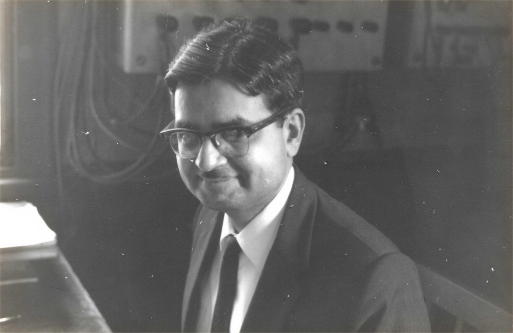
BS Sonde, retired professor of electrical communication engineering, was the founding chair of the Centre for Electronics Design and Technology (CEDT), renamed the Department of Electronic Systems Engineering in 2012. In this interview, he recalls why the need for CEDT was felt, and how it was founded with Swiss collaboration.
What were the developments from the Indian side that led to the establishment of CEDT?
It all started with the Bhabha Committee report. The Government of India had appointed Dr Homi Bhabha and a group of very distinguished scientists and technologists to the Committee [in 1963], to recommend what should be done in the country in the next five years in order to make better use of electronics. Electronics was becoming all-important, especially for national security, but we had done very little. It was pointed out that if we don’t take immediate measures we would be left in the lurch and others would score over us. Also, the electronics industry had to grow to bring in employment opportunities for our people, and we had to become self-sufficient. So for all these reasons the Committee gave its recommendations in 1966.
But Dr Bhabha died in an air crash in January that year. Dr S Bhagavantam, former Director of the Institute, who was Scientific Advisor to the Defence Minister at the time, completed the report on behalf of the Bhabha Committee. Soon thereafter the Government wanted to set in motion some things; the Department of Electronics was carved out to coordinate the efforts.
In 1970, the Government of India wanted to review what had happened to the Committee’s recommendations. So the government organised a week-long National Conference on Electronics at the Tata Institute of Fundamental Research, Bombay in March 1970. The Institute was invited to participate, and Prof Satish Dhawan, the Institute’s Director, put together a small delegation for the conference. Its members were Prof BS Ramakrishna, the head of the department of ECE [Electrical Communication Engineering]; myself; Prof G Suryan from Physics; Prof Joseph Vithayathil from Electrical Engineering; and then we had a visiting professor from the US, Prof Thomas Kailath. The conference had a session on education, in which industry people told us that the knowledge imparted to students in classrooms was not suitable for their requirements – they wanted the students to develop something new. They asked us to do something about it. We told them we cannot keep changing the syllabus too often and include industry-related requirements. We provide students with good knowledge, enough for them to move from one area to another easily, but the industry people felt that that is not enough – you have to make the students more practical.
When we came back, we started discussing this in the Institute in smaller groups. We found that there could be two routes – one route could be an entirely new programme on electronics design and other things. But if there is a change in the nature of the electronics industry, the students would find it difficult. The other route was to superpose a one-year design- and technology-oriented programme, meant for good people who are trained in the traditional way. This would give us a shorter turnaround time.
The industry people felt that we have to make the students more practical
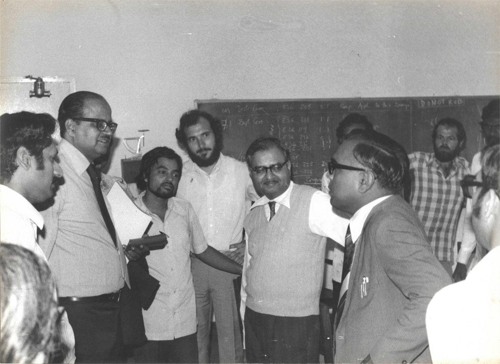
In that discussion, Prof Thomas Kailath was also present. He was a worldwide traveller. He said, “Look, I know Dr Arvind Shah [then at ETH Zurich]. He has also been talking of this, and planning similar things.” Similar problems were also arising in Switzerland because technology keeps changing so rapidly. The Swiss watch industry was getting into difficulties. Because of the progress in electronics and miniaturisation, conventional mechanical watches were being left out. So they were looking at how to give new training to people so that they can rejuvenate the industry. So Prof Kailath gave us the contact to Dr Shah. Shah came to India sometime later, and we had a short discussion here for a couple of hours, to begin with. We got some inputs from him and that was useful. He brought his plan, and we also had one.
With the help from the Chairman of the Electrical Sciences Division at that time, Prof BN Narayana Iyengar, I brought together people from industry for a discussion meeting at the Institute on what is to be done, and many people agreed that we can work out a one-year or a one-and-a-half year program, which will superpose on the BE degree. But how to bell the cat? First, we needed money. We required new equipment, new facilities and the like, and the Institute did not have funds at the time. We were getting just a couple of crores in a five-year period for any development work. Compared to the Institute’s prosperity today, in those days it was very difficult. Fortunately, Dr Shah contacted the Swiss Agency for Development and Cooperation [SDC], who could support the programme. And finally, the Governments of India and Switzerland signed an agreement in August 1974 to establish CEDT at the Institute. Prof Dhawan assigned me the responsibility of steering the programme.
Did the plan from the Institute match up with the plan that Arvind Shah had?
There were a lot of similarities because the goal was similar.
After CEDT was established, what was the nature of the exchange between the two sides?
First, laboratories and technology facilities had to be set up at the Institute. This costs money, and the SDC gave us a grant. The greatest advantage of this grant was that they said it was not necessary that we buy equipment and services only from Switzerland. But there was a need for a matching contribution, just like with any foreign collaboration. Fortunately, at that time, both the Electronics Commission and the UGC readily agreed to support this effort from the Indian government’s side.
How important was Swiss expertise?
It was very important. They brought good practical knowledge of state-of-the-art electronics equipment covering many areas: instrumentation, communication and industry needs. Also, the new facilities planned and procured had to be set up quickly to launch the new postgraduate diploma programme. All the Swiss experts actively participated in this work along with us. Besides, we could also receive orientation at Swiss institutions and industries under this programme. This helped create a strong base towards self-sustenance in chosen areas of electronics design and technology for the future.
In later years, the one-year postgraduate (PG) diploma programme gave way to MTech and PhD programmes. How and why did the focus evolve from being industry-focused to being more academic?
It happened because of the Institute’s environment and academic freedom. Also, as a national policy, the MTech programme duration was shortened to one-and-half years by early 1980s, from the earlier two years, which led to a growing clamour from the students – even those sponsored from industry – for MTech in preference to the PG diploma. At the same time, young faculty members at CEDT were keen to benefit from the research opportunities on campus and advance their careers. In the initial years, I was able to resist their temptation of taking up PhD research as we were building up CEDT, which required all their time and energy. However, in later years, it is creditable that many of our young faculty took up part-time PhD research at ECE, EE [Electrical Engineering] and other departments of the Institute, and did exceedingly well and became PhD supervisors themselves in later years. These measures also helped CEDT to receive the status of a department at the Institute many years later.
What would you say has been the enduring impact of CEDT on the electronics industry and electronics education in India?
CEDT has been a pacesetter for R&D activities in the electronics industry in India. The R&D personnel employed by the industry were not up to the expected mark until we came into the picture. That is the reason why the Government of India decided that there should be centres like CEDT elsewhere in the country. I had the opportunity to help the Department of Electronics in this activity. I am glad that many centres with our basic objectives are now functioning. Also, in 1985-86, we helped set up the Electronics Design Laboratory at Chulalongkorn University, Bangkok, under the UNDP [United Nations Development Programme] South-South Cooperation Programme with support from the Government of India.
CEDT has had an influence on electronics education too. Students at CEDT and elsewhere in India required learning material but it wasn’t always available at an affordable cost. So we had taken it upon ourselves, at the Institute, to write what we were teaching in a simple manner, with problem sets and the like. In fact, we were publishing such notes first in cyclostyle versions and later in print even before CEDT was set up. This experience was extended and expanded at CEDT and a wide range of learning material was published in the CEDT series. A good example is the book Printed Circuit Boards: Design and Technology, prepared by Walter Bosshart, our Swiss expert, which has become highly popular among students and industry users.