Amogh Kinikar, who did his Master’s in Physics at IISc, on why graphene is a fascinating material
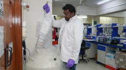
In 2012, I found myself in the Department of Physics at IISc, holding a five-and-a-half feet tall, extremely top-heavy object called a dip stick. It was a long narrow vacuum chamber that could be inserted into vessels containing cryogenic fluids. This particular one was made nearly two decades ago by Sohini Kar-Narayan, currently a faculty member at the University of Cambridge, during her PhD in the department. And in it was the apparatus which allowed me to measure electrical properties of the cleanest graphene flakes. I used a sharp metal tip to exfoliate graphene from its parent graphite crystal. Both the metal tip and the graphite crystal are conducting, so I could measure the graphene as it was being exfoliated, and because this graphene was not exposed to the air or any chemicals, it was as clean as graphene could get.
For the better part of the last century, many discoveries in physics — ranging from those about sub-atomic particles to the cosmos — have captured the public imagination. But in 2004, the relatively obscure field of condensed matter physics caught public attention with the discovery of a new form of carbon with extraordinary properties called graphene. In the years since, several superlatives have been used to describe the significance and implications of this discovery. But why is graphene so fascinating?
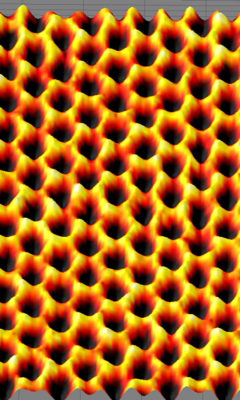
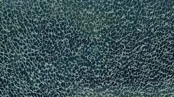
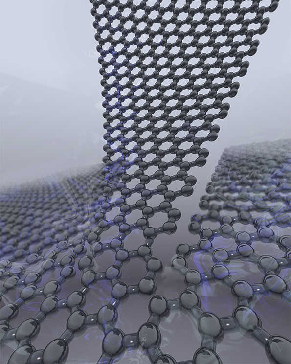
It was in the summer of 2003 that a scientist known for pushing the boundaries of materials science, Andre Geim at the University of Manchester, tasked his postdoctoral associate, Kostya Novoselov, with making the thinnest layer of graphite, a familiar crystalline material so soft that it is commonly used in pencil leads and solid lubricants. For the past thirty years, physicists all over the world have used graphite to calibrate microscopes (called scanning tunneling microscopes) which can see atoms, because graphite could be obtained in very high-quality crystals. To clean the surface of these graphite crystals, they would remove the top-most layer with a simple adhesive tape. The crystal was so soft, a thin layer of it would be exfoliated as the tape was peeled off. Novoselov took the next leap and peeled off another layer from the layer that was already stuck to the tape. He did this a few more times, ending up with a very thin layer of graphite — so thin that at a few places it was just a few atoms thick. And thus graphene was discovered. 1 Graphene was clearly a unique substance: it was the thinnest material ever made. And it had an uncomplicated structure, a hexagonal array of carbon atoms with each atom bonded to three other carbon atoms.
After its discovery, physicists worldwide began investigating its properties. IISc too has developed a rich association with graphene, having produced a few of the most cited papers in the field. Arindam Ghosh’s lab in the Department of Physics showed, in 2013, that graphene has the highest responsivity of any photodetector (it had the largest change in current produced per photon intensity). However, graphene by itself is very transparent, absorbing only 2.3% of the light that falls on it. To develop a photodetector, Kallol Roy, a student in Ghosh’s lab, placed graphene on top of another 2D material, molybdenum disulphide (MoS2). Unlike graphene, MoS2 absorbs light very well, but does not conduct electrons, something graphene is good at. So if you put one layer of graphene on top of a few layers of MoS2, you can combine the best of both worlds to get the highest responsivity from any photodetector.
IISc has developed a rich association with graphene, having produced a few of the most cited papers in the field
But one Institute member made a significant contribution to graphene research decades before it was actually discovered — this was none other than Sir CV Raman. Raman spectroscopy, based on the Raman effect, the discovery for which the physicist won his Nobel Prize, is one of the most widely used techniques in material and chemical sciences, and it finds extensive use in graphene research too. Over 20% of the research papers published on graphene in the year 2016 used the technique in some form. This is because Raman spectroscopy can be used to study the vibrations of materials as described by quantum mechanics. All objects constantly vibrate, and although these vibrations can be thought of like waves on a string, light interacts with them as though they were particles. This is the wave-particle duality of quantum mechanics. Using the Raman effect we can measure the frequency of these vibrations, and in these frequencies are fingerprints that reveal a material’s properties. A pioneering discovery in this field was made by Anindya Das when he was a graduate student in the Department of Physics, where he is now a member of the faculty. He was the first to demonstrate how applying an electric field changes graphene’s Raman spectrum. As Raman spectroscopy is a widely available and relatively straightforward technique, this discovery provided an easy way to characterise properties of graphene.
Amongst all its superlative properties, perhaps the best known is graphene’s strength — it is perhaps the strongest material known to humans. It has been claimed that a layer of graphene as thin as plastic cling-wrap is so strong that you would need to balance an elephant on top of a pencil to be able to pierce it. However, that statement needs to be taken with a tiny grain of salt. The strength measurements (which do not include elephants) were performed on tiny flakes of graphene, which are generally free from defects. And that is crucial because defects are the places where things begin to break. A defect-free sample would necessarily be much stronger than one with defects. The techniques currently used to make graphene on large scales, by chemical vapour deposition (CVD), leave a lot of defects in the graphene layer. But CVD graphene is the only feasible way to ensure the properties of graphene find applications; exfoliated graphene is prohibitively labour-intensive and expensive.
So how does CVD graphene fair in the elephant-on-a-pencil test? Not very well, it turns out. CVD graphene is very delicate, although there are ways to improve its strength. If you can remove certain kinds of defects it is nearly as strong as exfoliated graphene. But doing this on a large scale remains a challenge.
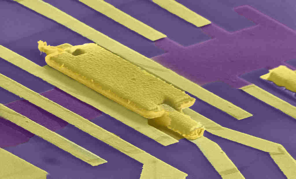
CVD graphene is also crucial for applications such as flexible or transparent electronics. It is not just the mechanical properties of graphene that are important in these applications, but also the electrical ones. Again, because of the defects, CVD graphene is not as good as exfoliated graphene, as each defect is an obstacle which scatters the electron from the path it was travelling on. But it is getting better. A different problem with CVD graphene may now have a solution, thanks to Mayank Shrivastava at the Department of Electronic Systems Engineering. When we put metal contacts on CVD graphene, the “contact resistance” is very high — it takes energy for the electron to leave the metal and jump into graphene. So if we were to make computer chips out of graphene, they would be very power-hungry because of the high contact resistance. Shrivastava has proposed a design that has the record lowest contact resistance. The key to its success lies in designing contacts with the right kind of defects, so that the electrons in those defect sites can easily jump into the metal and also into graphene. It replaces the barrier with a slide.
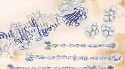
The Nobel Prize in Physics 2010 was awarded to Geim and Novoselov not just because they measured graphene devices. The prize also recognised paradigm shifts in our understanding of the material world. We suddenly had access to a two-dimensional material which was strong, absorbed little light, and could conduct electricity. A host of physics and chemistry thought experiments suddenly became practical. And even the most enthusiastic of graphene’s admirers will perhaps be surprised at the applications graphene is now finding in biology, which include using it as a drug delivery system or even as a biosensor. But its most revolutionary application yet may be in DNA sequencing. DNA is a very long and extremely narrow molecule — the width of a single strand of DNA would be similar to that of a few of graphene’s hexagons. A collaboration across various departments in IISc and the Jawaharlal Nehru Centre for Advanced Scientific Research (JNCASR) led by CNR Rao demonstrated, in 2008, how DNA nucleotides interact with the surface of graphene. Following this, Cees Dekker at TU Delft, Netherlands, showed in 2010 that if graphene had a tiny hole, you could thread the DNA through it and that it would be stabilised by its interactions with the graphene. If you were then measuring the current across the hole, depending upon what nucleotide was passing through, the value of the current would change. This allows for extremely rapid DNA sequencing.
Such advances have been made possible over the last decade because of graphene’s extraordinary properties. And it is in terms of mastery over materials that the stories of civilisations are often described, from the stone age to the silicon age. In time, graphene, whose superlative properties we are still trying to unsheath and wield, may usher in a new age.
1. Technically, it was rediscovered. The first experimental evidence and procedure to create graphene was documented in 1962 by Hanns-Peter Boehm. (The paper, in German, is here.) Despite being presented in an international conference and published in a widely-read journal, the discovery was ignored. The very modestly written paper made little of the fact that it was reporting the discovery of the thinnest material.↩